30+ fpga block diagram explanation
It is fully compatible with the STM32 System Bootloader and supports the same communication interfaces and commands and can also be used with. 016 to 350 MHz.
2
The Zynq-7000 architecture tightly integrates a dual-core 650 MHz ARM Cortex-A9 processor with Xilinx 7-series Field Programmable Gate Array FPGA logic.

. Heres an example sketch to write some data to the EEPROM. SE-block adaptively recalibrates the feature-maps of each layer by multiplying convolved input with the motif responses. Modular neural network computing apparatus are provided with distributed neural network storage.
Zybo Z7 Reference Manual The Zybo Z7 is a feature-rich ready-to-use embedded software and digital circuit development board built around the Xilinx Zynq-7000 family. 016 to 710 MHz HCSL. The block diagram down below indicates how a Counter Type ADC works Counter Type ADC Block Diagram Integrating Dual-Slope ADC An integrating ADC dual-slope ADC applies the analog input voltage to the input of an integrator and allows the voltage to ramp for a fixed time period the run-up period.
And the misuse of this block will result in different simulation and synthesis results. 8 to 30 MHz CMOS input. This pairing grants the ability to surround a.
5 to 710 MHz Independently configurable outputs support any frequency or format. Using employees in yellow belt roles. See the Skydel-SDX Folder section for a detailed explanation of each folders contents.
As a result of its layout RAID 4 provides good performance of random reads while the performance of random writes is low due to the need to write all parity data to a single disk unless the filesystem is RAID-4-aware and compensates for that. File Transfer Protocol. A CPU cache is a hardware cache used by the central processing unit CPU of a computer to reduce the average cost time or energy to access data from the main memory.
Arty Z7 Reference Manual The Arty Z7 is a ready-to-use development platform designed around the Zynq-7000 All Programmable System-on-Chip AP SoC from Xilinx. The Gray code counter used in this design is Style 2 as described in Cliff Cummings paper. A cache is a smaller faster memory located closer to a processor core which stores copies of the data from frequently used main memory locationsMost CPUs have a hierarchy of multiple cache levels.
It creates a conflict of interest between the yellow belt and green belt. 016 to 250 MHz CMOS. The FIFO counter consists of an n-bit binary counter of which bits n-20 are used to address the FIFO memory and an n-bit Gray code register for storing the Gray count value to synchronize to the opposite clock domain.
Guidelines for using always block The general purpose always block of Verilog can be misused very easily. Time you will find a Skydel-SDX folder inside your Documents folder. Yellow Belts tend to have less training and are less involved in six sigma and can only effectively support the logistical aspects of the project team.
元器件型号为SI5338C-B03792-GMR的类别属于半导体模拟混合信号IC它的生产商为Silicon Laboratories Inc官网给的元器件描述为点击查看更多. It is too costly. 5 to 200 MHz SSTLHSTL input.
The Intel FPGA design services team have developed a pool of expertise and a wealth of intellectual property IP to solve customer design challenges in the areas of intelligent video and vision processing. An advantage of RAID 4 is that it can be quickly extended online without. Connect the 30 dB attenuators to a DC-Block.
Languagec Include the Wire I2C Library include This address is determined by the way your address pins are wired. RAID 4 consists of block-level striping with a dedicated parity disk. Gray Code Counter.
Connect the DC-Block to the antenna port of the GNSS receiver. 016 to 200 MHz SSTLHSTL. Walk through the comments in the code for an explanation about whats going on.
The gating mechanism is exploited in SE-block using the sigmoid activation function which models the non-linear responses of the feature-maps and assigns a weight based on feature-map relevance Zheng et al. In this section the general guidelines are provided. 5 to 350 MHz Differential input.
Introduction ST Open Bootloader is example application code for STM32 microcontrollers providing In-Application programming IAP and is offered in the STM32Cube MCU Packages and GitHub. Engineering services offered include FPGA RTL design FPGA board design and system architecture design. What would be the best explanation for this perspective.
2022 USENIX Annual Technical Conference will take place July 1113 2022 at the Omni La Costa Resort Spa in Carlsbad CA USA. Pure sine wave inverter implementation and circuit diagram. USENIX ATC 22 will bring together leading systems researchers for cutting-edge systems research and the opportunity to gain insight into a wealth of must-know topics.
The Zynq family is based on the Xilinx All Programmable System-on-Chip AP SoC architecture which tightly integrates a dual-core ARM Cortex-A9 processor with Xilinx 7-series Field Programmable Gate. In the diagram from earlier we connected A0 and A1 to Ground and A2 to 5V. In various embodiments a neural inference processor comprises a plurality of neural inference cores at least one model network interconnecting the plurality of neural inference cores and at least one activation network interconnecting the plurality of neural inference cores.
I have got pure sine wave in my final year project hybrid pure sine wave inverter after connecting a LC filter at the output of H BridgeI have LC values L 2mH and C 33uf Diagram of pure sine I have got in my final year project is shown in figure below.
Fpga Cpu News Exploring Parallel Computer Architecture With Fpgas
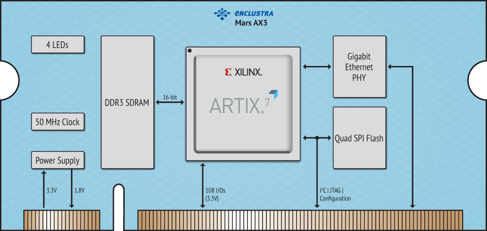
Enclustra Fpga Solutions Mars Ax3 Xilinx Artix 7 28nm Fpga Module 7a35t 7a50t 7a100t
2
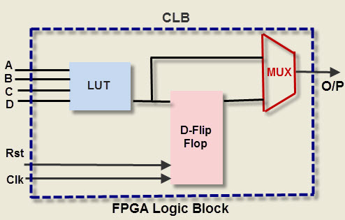
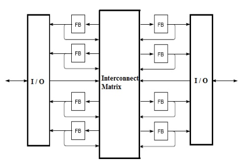
Know About Fpga Architecture And Thier Applications
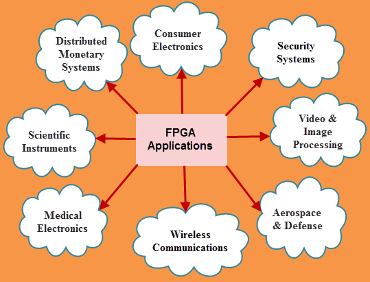
Know About Fpga Architecture And Thier Applications
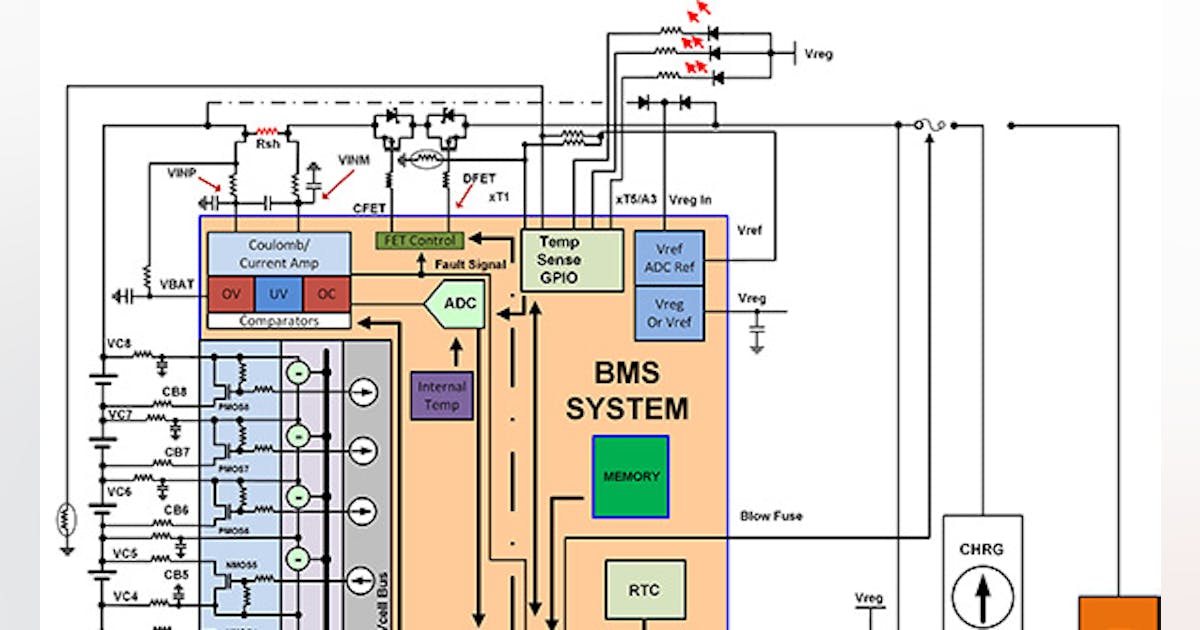
A Look Inside Battery Management Systems Electronic Design

Enclustra Fpga Solutions Mercury Ca1 Intel Cyclone Iv E Fpga Module Ep4ce30 Ep4ce75 Ep4ce115
Applications Of Complex Programmable Logic Device Cpld

Multi Resource Scheduling For Fpga Systems Sciencedirect
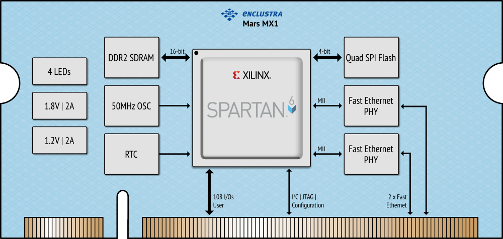
Enclustra Fpga Solutions Mars Mx1 Xilinx Spartan 6 Lx Fpga Module Xc6slx45
Know About Fpga Architecture And Thier Applications
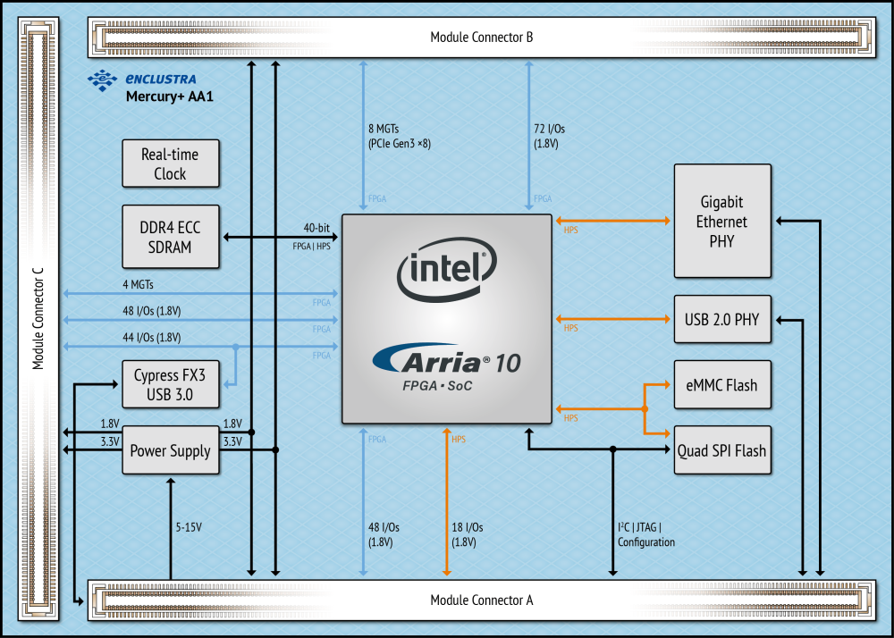
Enclustra Fpga Solutions Mercury Aa1 Intel Arria 10 System On Chip Soc Module System On Module Som 10as027e4 10as027e2 10as048e2 10as048e3

Fpga Cpu News Exploring Parallel Computer Architecture With Fpgas
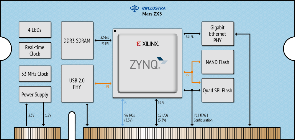
Enclustra Fpga Solutions Mars Zx3 Xiliny Zynq 7020 All Programmable System On Chip Soc Module System On Module Som Xc7z020
Know About Fpga Architecture And Thier Applications
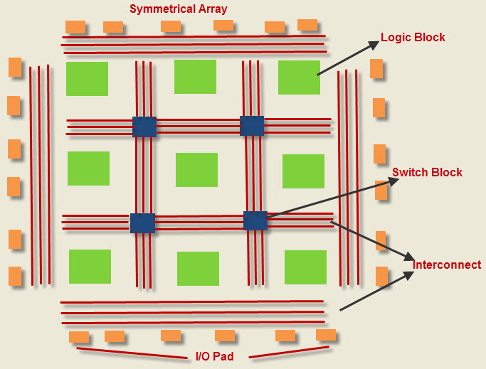
Know About Fpga Architecture And Thier Applications

Multi Resource Scheduling For Fpga Systems Sciencedirect